
Mold tooling and manufacturing
|
Short Description |
Manufacturing from mold to mass production and profer selection of material per application |
|
Description and feature list |
Transfer simulated design into mold design |
|
Proposed Engineering Service |
Mechanical design;consulting; Hardware design;system design |
|
Proposed Design Service |
System Architecture;Hardware Design;Verification;Testing;Certification;Quality Mgt; Consulting Manufacturing;Verification;Prototyping;End Customer Product Prototyping;End Customer Product Manufacturing;Mold tooling |
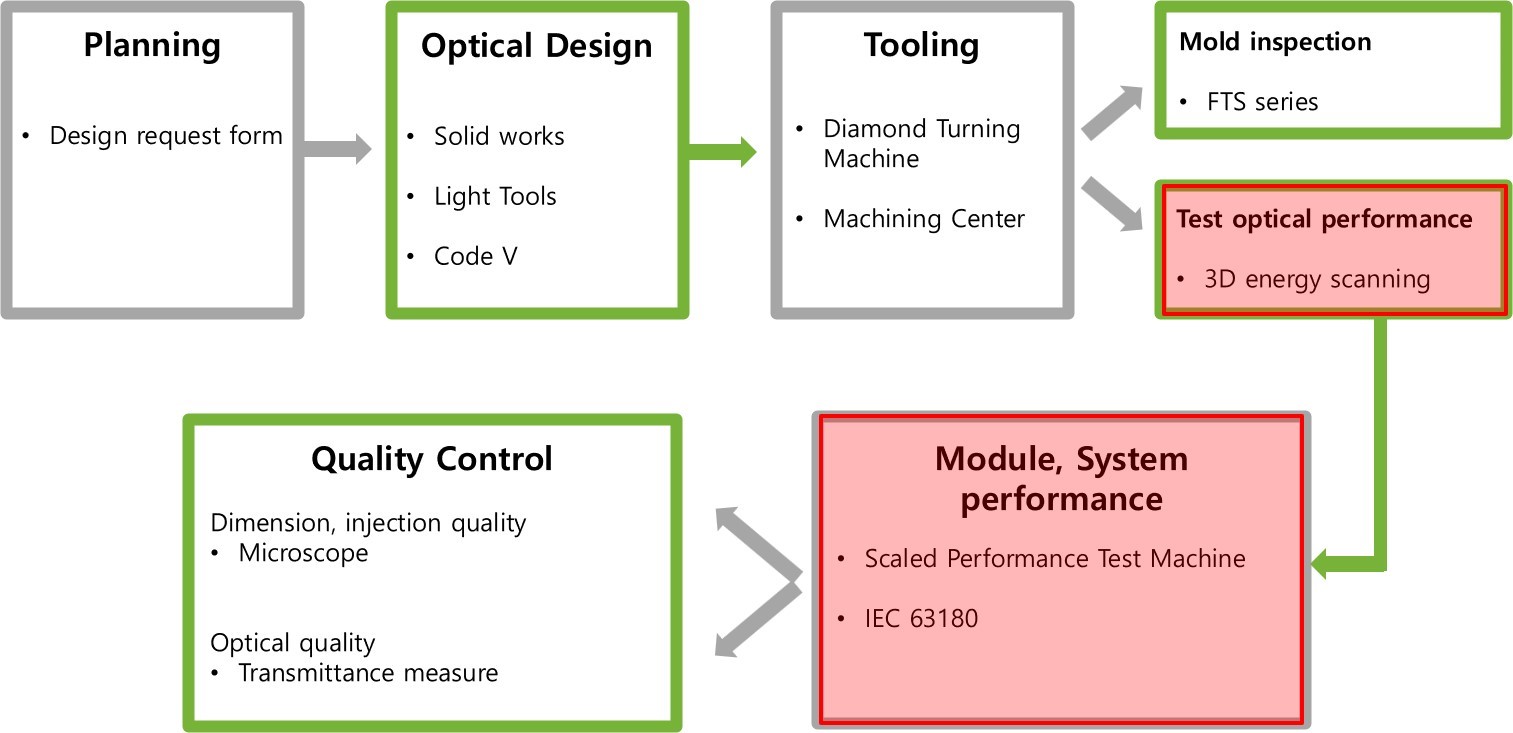
< General Design process of optics for TMOS sensor - Ref: Development process of Fresnel Factory Inc.>
This is a service that tooling and manufacturing to implement finished optical design into real life product. Please feel free to contact ashton@fresnelfactory.com for further question.
Typical service time is from 8 weeks to 16weeks.
Please check below information for better understanding what kind of “Mold tooling and manufacturing”
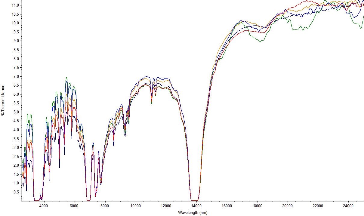
1. Choose high transmittance material for 8~13um wave length
2. Stable and less degradation material for the use case
3. Managing less than ±1mm tolerance in alignment sensor and optics
1. Choose high transmittance material for 8~13um wave length
Overall performance of device is combination of the performance of TMOS sensor and the performance of lens. One of main factor of the performance of lens is transmittance in Far infrared wavelength.
Device Performance = TMOS sensor * Lens transmittance rate
Typical FIR transmittance rate of black colored lens is less than 10% at FT IR measurement.
Despite the performance of the TMOS sensor being 100%, the final device's performance is only 7% due to a lens transmittance rate of 7%. Even if the sensor improves its performance by 50% every year, the final device can only achieve a 3.5% improvement in performance each year. Therefore, it is necessary to collaborate with companies that possess high transmittance rates materials. A high understanding of materials can greatly affect the final product.
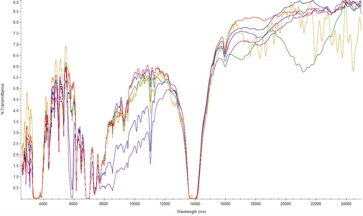
2. Choose stable and less degraded material for the use cases
To properly utilize the presence and temperature measurement functions of the TMOS sensor, it is important to choose materials with high transmittance rates, such as Poly FIR200. However, it is not enough to simply select materials with high transmittance rates. It is also necessary to understand how the transmittance and properties change due to additives used for production, such as pigments, anti-oxidization, and UV resistors.
There are materials available on the market, such as SBK150, which is already compounded as pellet contained pigments, anti-oxidization, and UV resistor. Selecting these materials can be a way to speed up development and reduce unnecessary costs.
3. Managing less than ±1mm tolerance in alignment sensor and optics
TMOS sensors are more sensitive to tolerance variations compared to PIR sensors. Generally, PIR sensors show satisfactory results at the ±0.2mm level of tolerance, while TMOS sensors can show satisfactory results in environments with tolerances of ±0.1mm or less. This difference is due to the difference in the size of the elements in each sensor.
Tolerance analysis is essential for ensuring that your design is robust and can be manufactured within the desired tolerances. It involves modeling the effects of post-molded shrinkage for plastic lenses on system performance and making design adjustments to minimize their impact. Lenses and housing tolerance must be correspondent to TMOS sensing element size, for example, tolerance for PIR sensor lenses is + 0.2 mm, but TMOS sensor has smaller size and it is recommended to decrease tolerances for Lenses and housings to +0.1 mm in order to maintain detector specification.
▶ News about FF’s manufacturing facilities for sensor optics
[FAQ]
1. What types of molds does Fresnel Factory provide?
- We offer both single-cavity and multi-cavity molds designed for high-precision optical parts. Depending on the project, we use diamond turning, nickel electroforming, or hybrid methods.
2. Why is diamond turning important?
- Diamond turning makes the mold surface extremely smooth and accurate, which helps create lenses with excellent optical performance and stable quality.
3. Can Fresnel Factory support high-volume production?
- Yes. For customers needing millions of parts each year, we recommend that ensure the highest durability and precision.
4. How do you ensure mold accuracy?
- We design molds with precise alignment systems, cooling structures, and optimized flow design. This makes it possible to mold very thin optical lenses reliably.
5. How are Fresnel Factory’s optical molds different from regular molds?
- Optical molds require extremely precise surface patterns that must remain stable over long production cycles. To achieve this precision, we use not only conventional machining centers but also Diamond Turning Machines (DTM) for ultra-fine pattern processing. In addition, the mold materials we select are stronger and more wear-resistant than those used in standard molds.
The optical core produced by DTM is then inserted into a mold base made with a machining center (MCT), completing a single high-precision mold assembly.
- Contact
USA : Frank Yim / frankyim@fresnelfactory.com
Global : Ashton / ashton@fresnelfactory.com